
A CPU begins as ordinary beach sand. By the time it reaches your computer, that sand has been refined into a crystal purer than almost anything in nature, sliced into wafers thinner than a fingernail, and had billions of microscopic switches printed onto it with light. The whole journey takes three to four months and passes through some of the most precisely controlled environments on earth.
Here is exactly how it happens, from raw material to finished chip.
Where a CPU starts: silicon from sand
Silicon is the second most abundant element in the Earth’s crust, found almost everywhere as silica — the main ingredient in sand. The problem is that naturally occurring silicon is nowhere near pure enough for electronics. Chip-grade silicon must be refined to 99.9999999% purity (nine nines), meaning fewer than one impurity atom per billion silicon atoms.
To get there, manufacturers heat quartz sand with carbon at extremely high temperatures to drive off oxygen. The result is metallurgical-grade silicon, which is then processed further using a series of chemical reactions that vaporize and re-condense the silicon until nearly every trace of other elements is gone.
Growing the crystal and slicing the wafer
Pure silicon is melted and seeded to grow a single, large crystal using the Czochralski process: a small seed crystal is dipped into the molten silicon and pulled upward, slowly rotating, as a cylindrical ingot forms around it. Modern ingots can be 300 mm (about 12 inches) in diameter and over a meter tall.
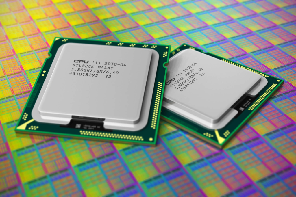
Once the ingot cools, diamond-tipped saws slice it into wafers roughly 0.75 mm thick. Each wafer is then lapped flat and polished to a mirror surface the tolerances involved are staggering. The wafer’s surface must be smooth to within a fraction of a nanometer, because any variation will distort the circuit patterns printed on top of it.
A single 300 mm wafer can yield hundreds of individual processor dies, depending on the size of each chip.
Designing the chip: what happens before fabrication
Before any silicon is touched in a factory, engineers spend years designing the chip. They map out the logical functions the CPU needs to perform, then translate that into a physical layout of billions of transistors and the metal wires connecting them.
This layout is encoded into a set of photomasks stencils, essentially, made of quartz and chrome. Each mask represents one layer of the final chip. A modern CPU may need more than 100 separate mask layers, and every one of them must align with the others to within a few nanometers.
Photolithography: printing circuits with light
Photolithography is the step that defines how small a chip’s features can be, and it is where the enormous cost of modern chips comes from.
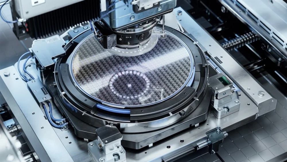
The wafer is coated with a material called a photoresist, which changes its chemical properties when exposed to light. A lithography machine then shines light through a mask, projecting a shrunken version of the circuit pattern onto the coated wafer. Where the light hits, the photoresist becomes soluble. A chemical wash removes those areas, leaving the pattern behind.
This sounds simple, but the light source is anything but. The most advanced chips use Extreme Ultraviolet (EUV) lithography, which produces light with a wavelength of just 13.5 nanometers shorter than a single DNA strand is wide. ASML, the Dutch company that makes these machines, is currently the only supplier in the world capable of producing them. A single EUV machine contains about 100,000 parts, ships in 40 freight containers, three cargo planes, and 20 trucks, and costs roughly $370 million. You can read more about the process on ASML’s own microchip manufacturing guide.
Key point: Even a chip built on TSMC’s 3nm process still uses older DUV (deep ultraviolet) lithography machines for most of its layers. EUV handles only the most critical, smallest features. The vast majority of patterning steps still run on DUV tools.
The photolithography step is repeated for every layer, with the wafer realigned precisely each time. One misaligned layer can ruin every chip on the wafer.
Doping, etching, and stacking layers
After each lithography step, two more processes shape the transistors: doping and etching.
Doping means firing atoms of other elements usually boron or phosphorus into the silicon at high velocity through ion implantation. These atoms alter how electrons move through the silicon, which is what makes transistors switch on and off. Different areas receive different dopants, creating the p-type and n-type regions that transistors need to function.
Etching removes unwanted material from the patterned areas using either chemical solutions or plasma. What’s left are the raised structures fins, gates, source and drain regions that form the transistors.
Once the transistor layer is built, the chip adds metal interconnect layers on top: thin wires of copper that connect transistors into circuits. A modern CPU can have 10 to 15 metal layers stacked above the transistors, each insulated from the next. The sequence of deposition, patterning, etching, and metal fill repeats for each layer, more than 1,000 distinct steps in total across the whole process.
Testing, binning, and why some cores get disabled
When all layers are complete, the wafer goes to electrical testing. Automated probes touch each die and run through thousands of checks. Defective dies are marked.
What happens next depends on yield the percentage of dies on a wafer that work correctly. For a chip with a small die area, yields are high. For a large die, even a tiny number of random defects can render a significant fraction of chips useless. TSMC reported an average yield of around 80% for 5nm test chips with a die area of roughly 18 mm², but that figure drops sharply as die size grows.
Chips that pass testing are binned sorted by how well they perform. A die that functions but can’t hit the top clock speed gets sold as a lower-tier model. A die with one defective core gets sold with that core disabled, rather than being discarded entirely. This is why a single production line can produce a whole family of CPUs at different price points from identical raw material.
Packaging: putting the die in a case
A bare silicon die is too fragile and too small to handle or connect to a circuit board. Packaging protects it and makes it usable.
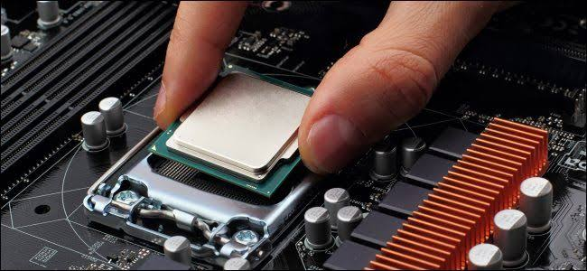
The die is attached to a substrate a small circuit board that routes the die’s electrical contacts to a larger grid of pins or solder bumps. Then a metal lid called an Integrated Heat Spreader (IHS) is placed on top, filled with thermal interface material to help transfer heat to a cooler.
Packaged chips go through a second round of testing — because bonding wires or solder connections can introduce new failures — before being stamped with their model number and boxed for shipping.
What ‘3nm’ actually means
When you see a chip described as ‘3nm’ or ‘4nm’, that number is not a physical measurement of any feature on the chip. The actual gate lengths on a ‘3nm’ chip are typically 12 to 30 nm. The node name became decoupled from physical dimensions around 2011 when transistors moved to three-dimensional FinFET structures, making a single length measurement too simple to capture the real improvements.
Today, node names are marketing labels that signal a generation of improvement usually meaning more transistors per square millimeter, lower power at the same speed, or both. TSMC’s N3 process, for example, offers roughly an 18% speed gain and 32% lower power compared to its 5nm process. Those are real improvements; the ‘3’ is just an index, not a ruler.
CPU manufacturing stages at a glance
| Stage | What happens | Key fact |
| Silicon refining | Sand is purified to 99.9999999% purity | Fewer than 1 impurity per billion atoms |
| Crystal growth | Czochralski process grows a silicon ingot | Ingots can exceed 1 meter in length |
| Wafer slicing | Ingot is cut into ~0.75 mm wafers and polished | One 300 mm wafer yields hundreds of dies |
| Photolithography | Light projects circuit patterns onto the wafer | EUV machines cost ~$370 million each |
| Doping & etching | Atoms are implanted; unwanted material removed | Creates the transistors’ switching regions |
| Metal interconnects | Copper wires connect transistors across 10–15 layers | More than 1,000 total process steps |
| Testing & binning | Probes check each die; sorted by performance | Yields ~80% on small dies; lower for large |
| Packaging | Die is mounted on substrate; heat spreader added | Second testing round before shipping |
Frequently asked questions
How long does it take to manufacture a CPU?
From the moment a silicon wafer enters a fabrication facility to a finished, packaged chip, the process takes around three to four months. Advanced nodes on the cutting edge of process technology can stretch to five or six months due to the sheer number of steps involved.
What is a silicon wafer and why is it used?
A silicon wafer is a thin disc of ultra-pure crystalline silicon that acts as the foundation for chip manufacturing. Silicon is used because it’s a semiconductor — its conductivity can be controlled precisely by adding small amounts of other elements and because it’s extremely abundant and relatively inexpensive to obtain.
How many transistors does a modern CPU have?
High-end consumer CPUs today typically contain 10 to 80 billion transistors, depending on die size and process generation. Apple’s M-series chips and AMD’s high-core-count server processors sit at the upper end of that range. The transistor count has roughly doubled every two to three years for decades, a trend known as Moore’s Law.
Who actually manufactures CPUs?
Intel manufactures its own chips at its own fabs. AMD, Apple, Qualcomm, and Nvidia are fabless — they design chips but outsource manufacturing, primarily to TSMC in Taiwan and Samsung in South Korea. TSMC alone produces the majority of the world’s most advanced chips, with a particularly large share of the high-performance CPU and GPU market. See ASML’s overview of the chipmaking industry for more on how the supply chain fits together.
Why are chips so expensive to manufacture?
The capital cost is enormous. A single advanced fab costs $20 billion or more to build. The lithography machines alone run into the hundreds of millions per unit, and the cleanrooms they sit in must maintain near-zero dust particles per cubic meter of air — about 10,000 times cleaner than outside air. Any contamination at any stage can destroy the chips on an entire wafer.
Conclusion
A CPU is sand that has been transformed into one of the most precise objects humans have ever built. The process runs from raw silicon through crystal growth, wafer preparation, hundreds of rounds of light-based patterning, doping, etching, and metal wiring before chips are tested, sorted, and sealed in their cases. The whole journey takes around three to four months and demands tolerances tighter than any other mass-manufactured product. Next time you see a ‘3nm’ chip announced, you now know both what goes into it — and what that number does and doesn’t mean.
Recommended Articles:
How to Test the Thermal Lottery on a CPU
How to Clear CPU Cache (and What Actually Speeds Up a Slow PC)