
A CPU schematic is a labeled diagram that shows the parts inside a processor and the wires that connect them. It maps out the control unit, the arithmetic logic unit, the registers, and the buses, so you can see how a chip takes in instructions and turns them into results.
Most of the time, when people search for this, they want the big-picture version: a clean drawing with a handful of labeled boxes and arrows. That is the kind of diagram this guide walks through. By the end, you will be able to look at one and understand what each part is doing and how data moves between them.
What is a CPU schematic?
A CPU schematic is a drawing of what sits inside a central processing unit, the chip that runs the programs on your computer or phone. It shows the working parts as blocks and uses lines to show how signals travel from one part to the next.
The point of the diagram is to make an invisible thing visible. A real processor packs billions of transistors into a piece of silicon smaller than a fingernail. You cannot follow that by eye. A schematic strips away the crowd and keeps only the parts that matter for understanding, so the whole design fits on one page.
These diagrams show up in textbooks, on exam papers, in course notes, and in hobby projects where someone builds a working processor from scratch. Same idea in each case: a simple map of a complicated thing.
Block diagram or full schematic? They are not the same
Two different drawings both get called a CPU schematic, and mixing them up is where confusion starts.
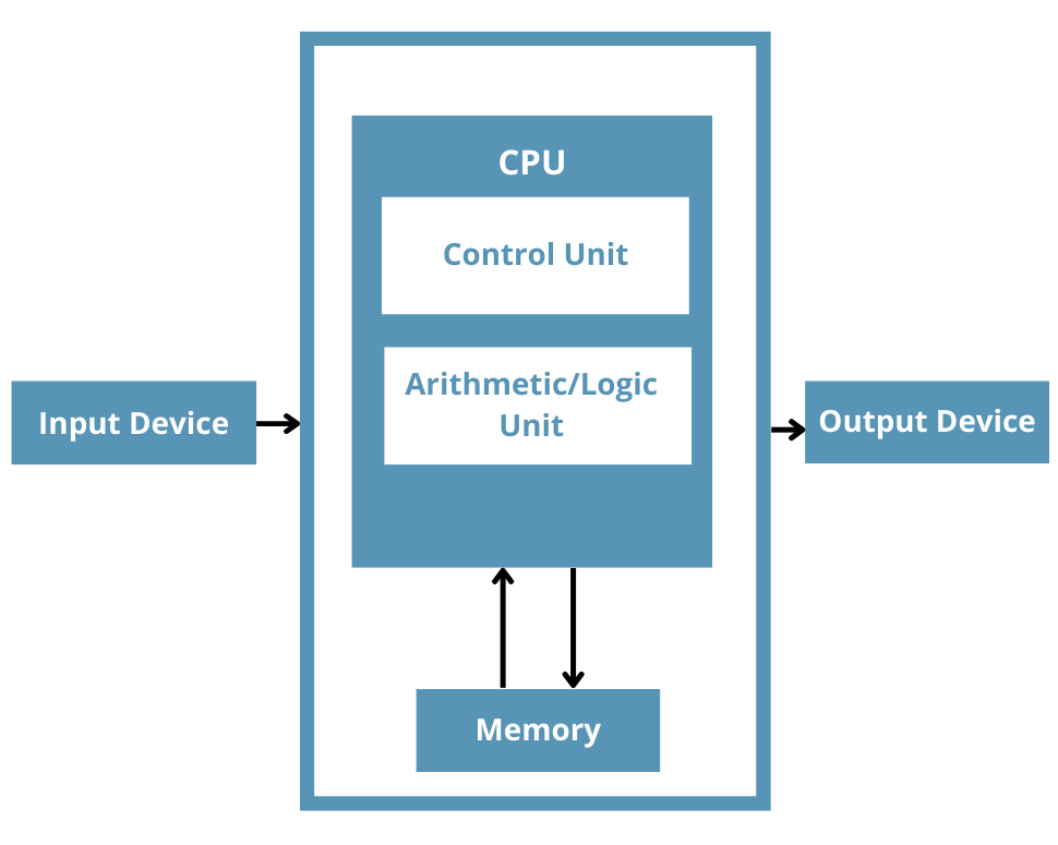
A block diagram is the high-level view. Each box is a whole function, like the ALU or the register file, and the arrows show the general path data takes. It answers the question, what are the parts and how do they connect? This is what most courses and articles mean, and it is what you picture when you imagine a CPU diagram.
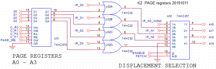
A full schematic is the detailed view. It shows the actual logic gates, chips, and individual wires needed to build the thing. A real one can run to dozens of pages. You would use it to build a processor, not just to learn how one works.
Quick rule: if the boxes are named after jobs (control unit, ALU), you are looking at a block diagram. If they are named after chips and gates (74HC181, a NAND gate), you are looking at a true schematic.
For learning how a CPU works, the block diagram is the right tool. It is clear, it fits on one page, and it shows the ideas without burying them in wiring. So that is what the rest of this guide focuses on.
The main parts of a CPU diagram
Nearly every CPU block diagram is built from the same short list of parts. Learn these seven and you can read almost any version you come across.
| Part | What it does |
|---|---|
| Control unit (CU) | Reads each instruction, works out what it means, and sends timing signals to every other part so the steps happen in the right order. |
| Arithmetic logic unit (ALU) | Does the actual math and logic: add, subtract, compare, AND, OR, and shifts. Two numbers go in, one result comes out. |
| Registers | Tiny, very fast storage slots inside the chip that hold the numbers being worked on right now. |
| Program counter (PC) | Holds the memory address of the next instruction. It steps forward on its own after each fetch. |
| Instruction register (IR) | Holds the instruction the CPU is working on at this moment. |
| Buses | The wires that carry data, addresses, and control signals between all the parts of the chip. |
| Clock | A steady pulse that keeps every step in sync, like a drummer setting the beat for the whole chip. |
Two of these do the heavy lifting. The control unit is the manager: it does not do the math itself, it just makes sure every other part acts at the right moment. The ALU is the worker: it takes two numbers and produces a result. Everything else exists to feed those two, hold their inputs and outputs, and move signals around.
You will often see registers split into named ones. The program counter and the instruction register are the two you meet first, and they matter enough that the next section follows them step by step.
How data flows: fetch, decode, execute
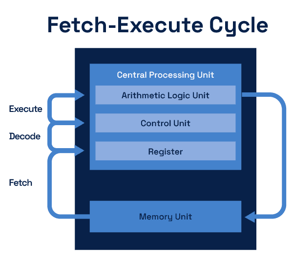
A CPU diagram is not just a parts list. The real value is watching how a single instruction travels through it. Processors repeat one loop over and over, millions of times a second, and it has three steps: fetch, decode, execute.
Say the program wants to add two numbers. Here is what the diagram shows happening:
- Fetch. The program counter holds the address of the next instruction. That address goes out to memory, the instruction comes back, and it lands in the instruction register. The program counter then steps forward on its own, ready to point at the next one.
- Decode. The control unit reads the instruction sitting in the instruction register and works out what it means. An instruction is really two parts: an opcode that says what to do (add), and operands that say what to do it with (these two numbers). The control unit turns this into a set of signals for the other parts.
- Execute. The control unit’s signals route the two numbers into the ALU, tell it to add, and send the answer to a register. The job is done, and the loop starts again with the next instruction.
This loop is called the fetch-decode-execute cycle, and it is the single most useful thing to understand about a processor. Once you can trace it on a diagram, the arrows stop being random lines. Each one has a job: this wire carries the address, that one carries the instruction back, this bundle carries the control signals.
Modern chips add clever tricks on top, working on several instructions at once and guessing what comes next to save time. But underneath, they still run this same basic cycle. If you understand the loop, you understand the core of every processor ever made. For a wider tour of how processors grew from this simple idea, Wikipedia’s central processing unit page is a solid next read once the diagram makes sense.
Where to find or draw a CPU schematic
If you want to see real diagrams or make your own, you have a few good options depending on how deep you want to go.
To learn from a diagram, start with the block diagrams in any computer architecture textbook or course notes. They all use the same parts, so once one clicks, the rest are easy. Drawing your own is one of the best ways to make it stick: put down the seven parts, then draw the arrows for a single add instruction and follow the cycle through.
To draw a clean version, a free tool like draw.io or any diagramming app works well. Use labeled rectangles for the parts and arrows for the buses. Keep it to the core blocks at first. You can always add detail once the basic shape makes sense.
To see a real, buildable schematic, look at a project that constructs a working processor from simple chips. Ben Eater’s
8-bit computer build is the best-known example. It comes with full schematics and video walkthroughs, and it shows how the tidy blocks in a diagram turn into actual wired-up hardware. Seeing both side by side, the simple block diagram and the real schematic, is what makes the whole thing finally connect.
Whichever route you take, the goal is the same: get to the point where you can glance at a processor diagram and narrate what each part does and where the data goes. That skill carries over to every CPU, from a beginner’s 8-bit build to the chip running the device in your hand.
Frequently asked questions
Is a CPU schematic the same as a CPU block diagram?
Not quite. A block diagram shows the parts as labeled boxes and is meant for learning. A full schematic shows the actual gates, chips, and wires and is meant for building. Most diagrams people call a CPU schematic are really block diagrams.
What are the main parts shown in a CPU diagram?
The core parts are the control unit, the arithmetic logic unit (ALU), registers, the program counter, the instruction register, buses, and the clock. The control unit directs traffic and the ALU does the math, while the rest store data and move signals around.
What is the fetch-decode-execute cycle?
It is the loop a CPU repeats for every instruction. It fetches the instruction from memory, decodes what it means, then executes it using the ALU. The processor runs this cycle millions of times a second to work through a program.
What is the difference between the control unit and the ALU?
The control unit reads instructions and tells the other parts when to act, but it does not do calculations itself. The ALU is the part that actually does the math and logic, taking two numbers and producing a result.
How can I draw my own CPU schematic?
Use a free tool like draw.io. Add labeled boxes for the seven core parts, then draw arrows for the buses connecting them. Start with just the main blocks, and trace one instruction through to check the flow makes sense.
Conclusion
A CPU schematic is a labeled map of a processor: the control unit, ALU, registers, program counter, instruction register, buses, and clock, plus the wires between them. For learning, you want the block-diagram version, not a full gate-level one. Get comfortable with the seven core parts, then trace a single instruction through the fetch-decode-execute cycle. Once you can do that, you can read almost any CPU diagram and explain exactly what is going on inside the chip.
Recommended articles:
The Most CPU-Intensive Games You Can Play Right Now
CPU Core Unpark: What It Does and How to Turn It Off in Windows
MS Office Click-to-Run High CPU: Why It Happens and How to Fix It
Windows Explorer High CPU: Why It Happens and How to Fix It
How to Find CPU Usage in Linux: 6 Commands That Actually Work